MOSFET stands for metal-oxide-semiconductor field-effect transistors. MOSFETs have four terminals: a source, gate, drain, and body/substrate. The body is assumed to be shorted with the source. The MOSFET is made of a single p-type Si wafer with doped n-type substrate at the source and drain, as well as metal contacts at the source, drain, and body. The gate spans the area above the source and drain, and is in contact with both regions. The gate consists of a thin silicon dioxide insulating layer(thickness ) between the metal and the semiconductor, hence the name “metal-oxide-semiconductor.” The name “field-effect” stems from the movement of charges within MOSFETs through drift current.

Channel Formation
Due to the properties of doped semiconductor regions, a depletion region forms between the n-regions and p-region. When all terminals are grounded, there is no current flowing for . However, when a positive voltage is applied to the gate, then majority holes under the gate are repelled and bound negative charges are revealed. Additionally, the positive voltage also attracts electrons, forming an n-type channel below the gate where current can flow. Thus, the p-type substrate below the gate is inverted.
Triode Region
I-V relation is curved as channel resistance increases with .
Lateral (drain-source electric field)
Electron drift velocity
Triode Resistance
Saturation Region
Increasing causes a widening of the depletion region near the drain, leading to a decrease in channel thickness in the region.
PMOS
Similar to NMOS but with reversed doping and voltage polarities. The two are complementary. In the PMOS symbol, the source arrowhead points into the MOSFET, or the base arrowhead out of the MOSFET. and are always negative.
| Name | Equation | Info |
|---|---|---|
| Oxide capacitance | ||
| Aspect ratio | ||
| Process transconductance | ||
| Transconductance parameter | ||
| Threshold voltage | Required to invert channel region Typically to | |
| Effective/overdrive voltage | NMOS PMOS | |
| Device parameter | ) | Depends on process parameters Smaller MOFSET lengths are greater |
| Channel charge | ||
| Operating regions and Current Equations |
| Operating Region | NMOS Conditions | NMOS Current | PMOS Conditions | PMOS Current |
|---|---|---|---|---|
| Cutoff | ||||
| Triode | For , negligible | For , negligible | ||
| Saturation | ||||
| Always |
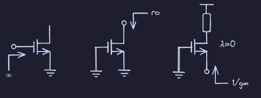
Small Signal Model
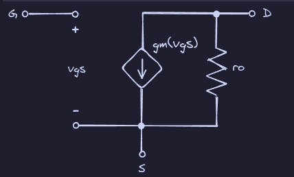
Transconductance
Output Resistance
Topologies
See: Transistor Amplifier
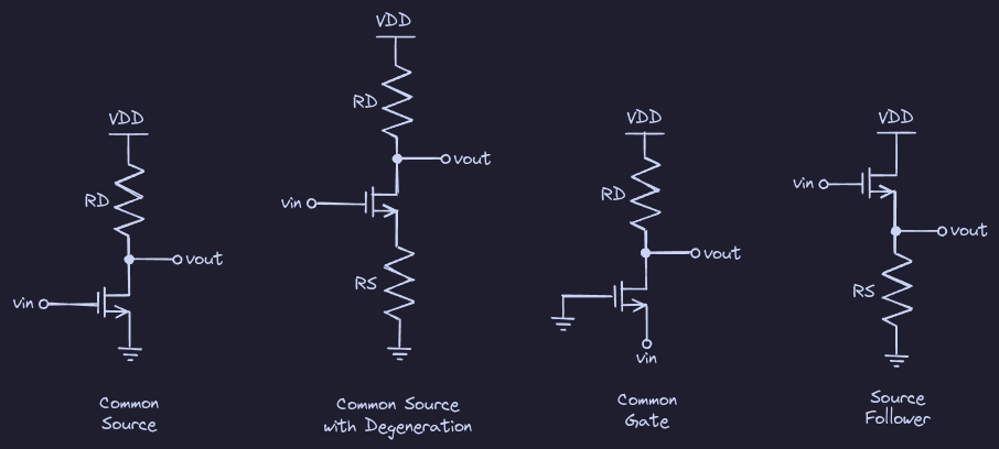
| Name | |||
|---|---|---|---|
| Common Source | |||
| Common Source with Degeneration | |||
| Common Gate | |||
| Source Follower |
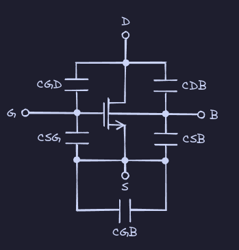
Parasitic Capacitance
See: Miller Theorem